1. Вступ
This manual provides essential information for the proper use and care of your Aexit Single-Sided Prototyping Boards. These boards are designed for building prototypes of electronic circuits, offering a reliable platform for your projects.
Each board measures 8 x 8 cm (3.1 x 3.1 inches) and features standard 0.1-inch industrial quality spacing for component mounting. The single-sided copper PCB is treated for easy soldering and extended shelf life, with referencing numbers printed on both sides for convenient identification of individual holes.
2. Особливості продукту
- Назва продукту: Плата PCB
- Діаметр отвору: Approximately 1mm / 0.04"
- Крок отвору: Approximately 2.54mm / 0.1"
- Розмір плати: 8 x 8cm / 3.1" x 3.1" (Length x Width)
- Товщина: Approximately 1.5mm / 0.059"
- колір: Синій
- матеріал: FR-4
- Вага нетто: 39g (for the package content)
- Вміст пакету: 2 x Universal PCB Board
- Single-sided copper PCB for easy prototyping.
- Referencing numbers printed on both sides for convenient hole identification.
- Treated surface for improved solderability and extended shelf life.
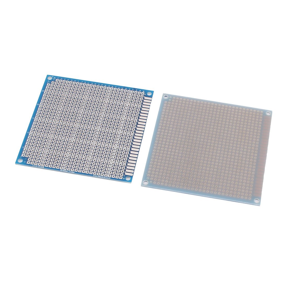
Figure 1: Aexit Single-Sided Prototyping Board (8x8cm).
This image shows the blue FR-4 prototyping board with its grid of holes, designed for mounting electronic components. The board's dimensions are 8x8cm, and it features clear markings for easy component placement.
3. Налаштування
Before beginning your project, ensure you have all necessary components and tools, including:
- Electronic components (resistors, capacitors, ICs, etc.)
- Паяльник і припій
- Різаки та зачистки дроту
- Multimeter for testing
- Захисні окуляри
Приготування:
- Plan your circuit layout on paper or using a software tool before placing components on the board.
- Identify the desired holes for each component using the printed referencing numbers.
- Ensure your workspace is clean, well-lit, and well-ventilated.
4. Інструкція з експлуатації
These prototyping boards are designed for manual assembly of electronic circuits. Follow these general steps:
- Розміщення компонентів: Insert component leads into the desired holes on the board. Bend the leads slightly on the solder side to hold the component in place.
- пайка: Heat the component lead and the copper pad simultaneously with the soldering iron. Apply a small amount of solder to the heated joint, allowing it to flow evenly around the lead and pad. Remove the solder and then the iron.
- Сполучні компоненти: Use jumper wires or solder bridges to connect different points on the board according to your circuit diagram.
- Обрізка проводів: After soldering, trim any excess component leads using wire cutters to prevent short circuits.
- Тестування: Before applying power, thoroughly inspect all solder joints for bridges or cold joints. Use a multimeter to check for continuity and short circuits.
- Застосування живлення: Once verified, apply power to your circuit. Monitor for proper operation and any signs of malfunction.
Примітка: Always exercise caution when working with electricity and hot soldering irons.
5. Технічне обслуговування
To ensure the longevity and reusability of your prototyping boards:
- Прибирання: After soldering, you may clean the board with isopropyl alcohol and a soft brush to remove flux residue. Ensure the board is completely dry before use.
- Зберігання: Store unused boards in a dry, dust-free environment, preferably in anti-static bags, to prevent oxidation and contamination.
- Розпаювання: When removing components, use a desoldering pump or wick to minimize damage to the board's pads.
6. Вирішення проблем
If your circuit does not function as expected, consider the following common issues:
- No Power/Incorrect Function:
- Check all power connections and ensure correct voltage і полярність.
- Verify all components are correctly oriented (e.g., diodes, ICs).
- Inspect for cold solder joints (dull, lumpy appearance) or solder bridges (solder connecting unintended pads).
- Use a multimeter to check for continuity where expected and for shorts where not expected.
- Пошкодження компонента:
- Ensure components were not overheated during soldering.
- Verify component values (e.g., resistor color codes, capacitor markings).
- Переривчаста робота:
- Check for loose connections or cracked solder joints.
- Ensure wires are securely connected and not frayed.
7. Технічні характеристики
| Особливість | Деталь |
|---|---|
| Торгова марка | Вихід |
| Номер моделі | модель |
| ASIN | B07F15NFVZ |
| Назва продукту | Плата PCB |
| Діаметр отвору | Approx. 1mm / 0.04" |
| Крок отвору | Approx. 2.54mm / 0.1" |
| Розмір плати | 8 x 8cm / 3.1" x 3.1" (L*W) |
| Товщина | Approx. 1.5mm / 0.059" |
| Колір | Синій |
| матеріал | FR-4 |
| Net Weight (Package) | 39г |
| Вміст пакета | 2 x Universal PCB Board |
| Дата першої доступності | 25 червня 2018 р |
8. Гарантія та підтримка
Aexit products are manufactured to high-quality standards. For specific warranty information or technical support, please refer to the retailer's return policy or contact Aexit customer service through their official channels. Keep your purchase receipt for warranty claims.
Для отримання додаткової допомоги, будь ласка, зверніться до офіційного представника Aexit. webсайт або зверніться до місця придбання.